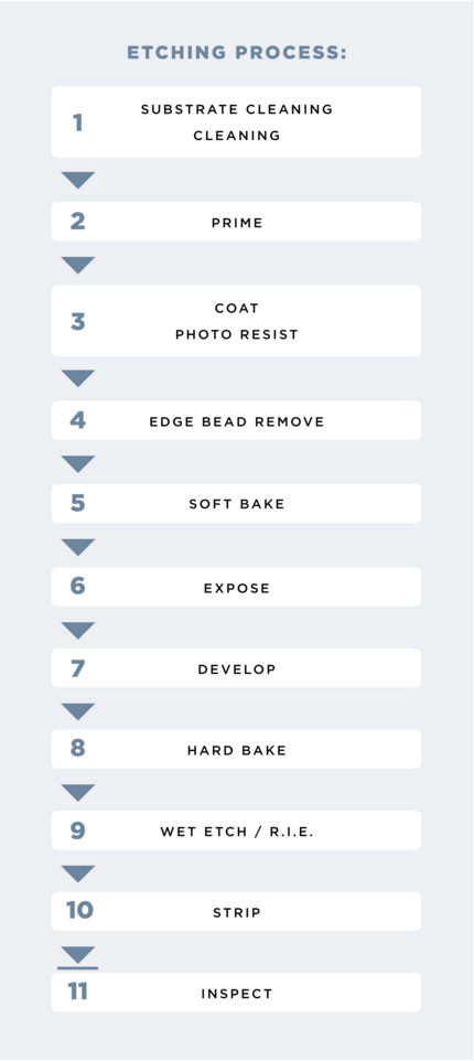
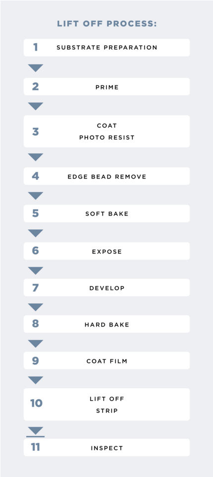
1. Photo Etch & Patterning:
Photolithography patterning is provided on almost all coating products of TFD. Metals such as Al, Al:Cu, Cr, NiCr, Ni, Au, Pd, Pt, Ag, Cu, Mo, Mo:Cr and many other alloys and oxides like I.T.O., IMITO™, & Black Cr. (Cr203). These are patterned as small as 2 micron resolution with sharp and tapered edges on up to 370 mm x 470 mm glass and other wafer substrates, 150, 200, & 300 mm.
Quality is ensured for all patterns. No residual coating remains in etched areas as small as 2 microns. The Plastic substrates are also patterned but to a lesser Resolution, 10µm features. Numerous display panels and IC masks are products requiring this high-quality patterning.
2. Patterned Products:
TFD has routinely fabricated multilayered products with Thin films as below:
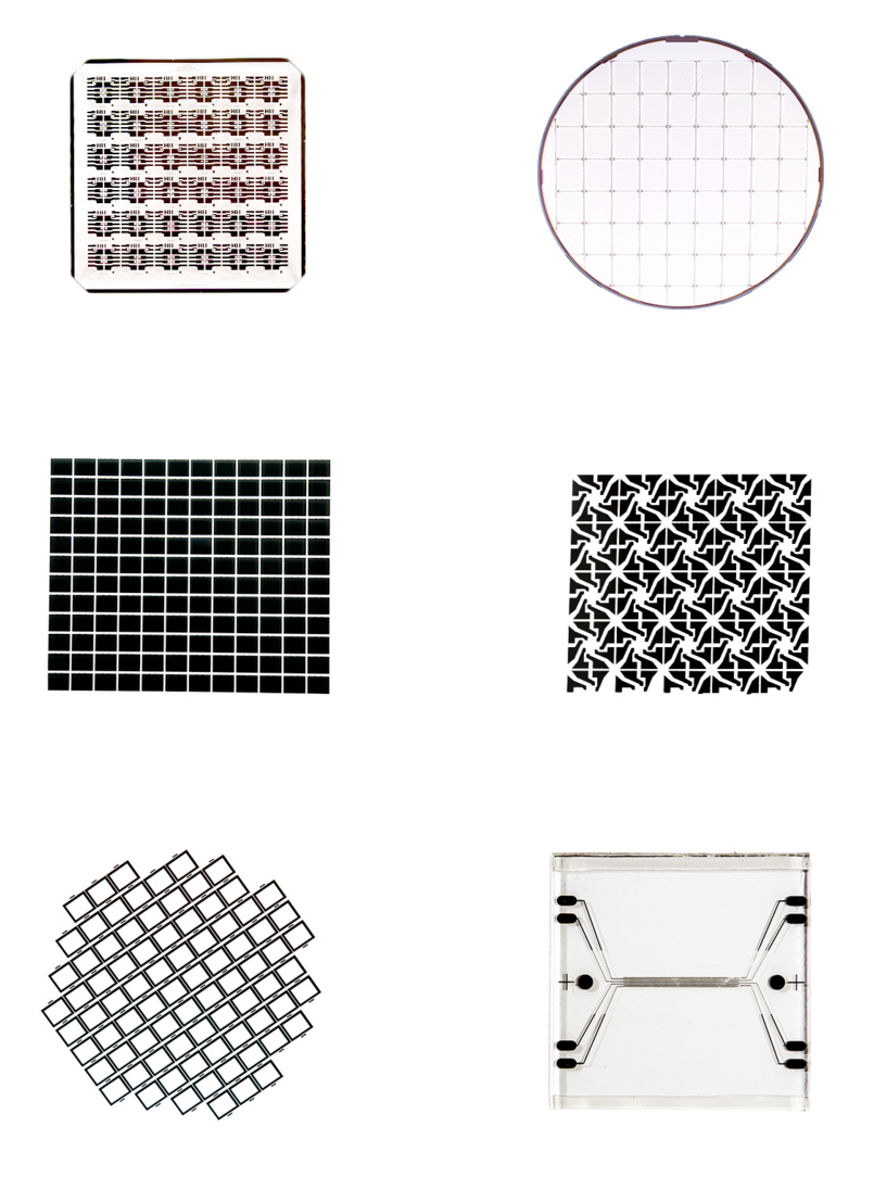
| PRODUCTS | LAYERS |
|---|---|
| a. Capacitive Touch Displays | I.T.O./I.M.I.T.O.™/Dielectric & Metal. |
| b. MEM – Display | Metal/Oxide/Metal |
| c. OLED – Display | I.T.O./Metal/Dielectric |
| d. Solar (Organic) | I.T.O./Metal |
| e. Solar (SIG) | Mo/I.T.O./Dielectric |
| f. Heater for (I-R region) | NiCr/Al:Cu & Ag:Au |
| g. Black Mask | Black Cr/Black Resist. |
| h. Other Products for Research & Development. |