I.M.ITO™, a multi-layer coating stack, was invented by Saleem Shaikh at Thin Film Devices in 1987. I.M.ITO™ was developed primarily to reduce internal and external reflections of I.T.O. when used in displays such as TFT-LCD, Chroma Filters, E.M.I. Shields and Heaters, when used with (primarily) LCD and others.
The I.M.ITO™ concept was first extended to Oled, Photo Voltaic, LCoS, Capacitive Touch Panels, and many other applications.
The use of the I.M.ITO™ concept has revolutionized the improvement of displays, and touch screen enhancements for sunlight viewability and superior contrast. Thin Film Devices, Inc. not only invented and developed I.M.ITO™ (Index Matched Indium Tin Oxide™), but also incorporated it with Ion-beam Sputter to produce much more superior and reliable coatings when compared to the Ion Assist evaporation process.
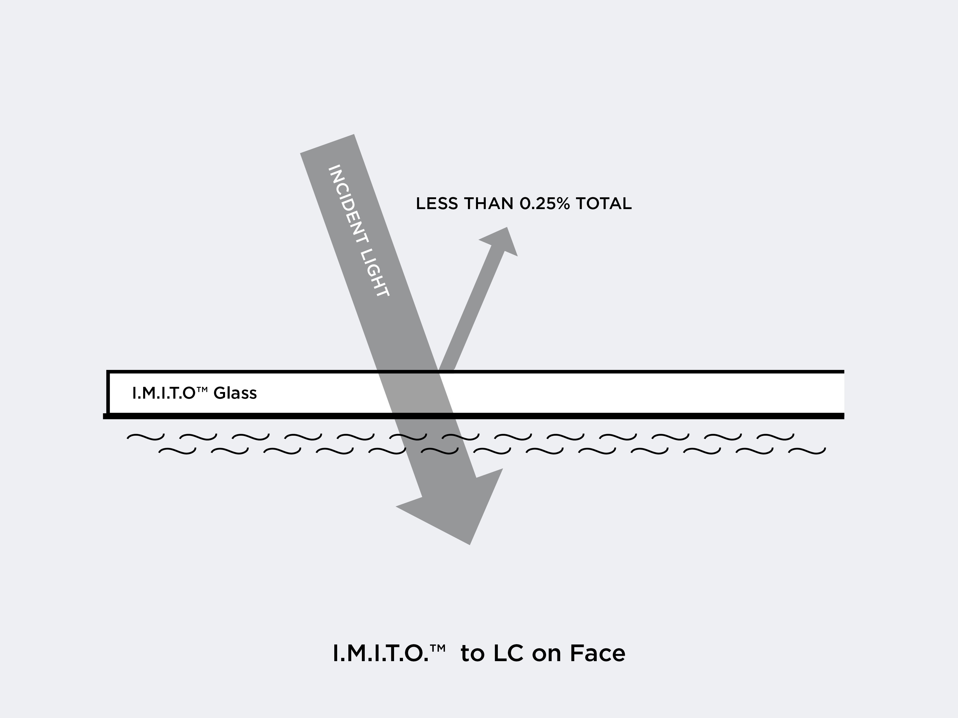
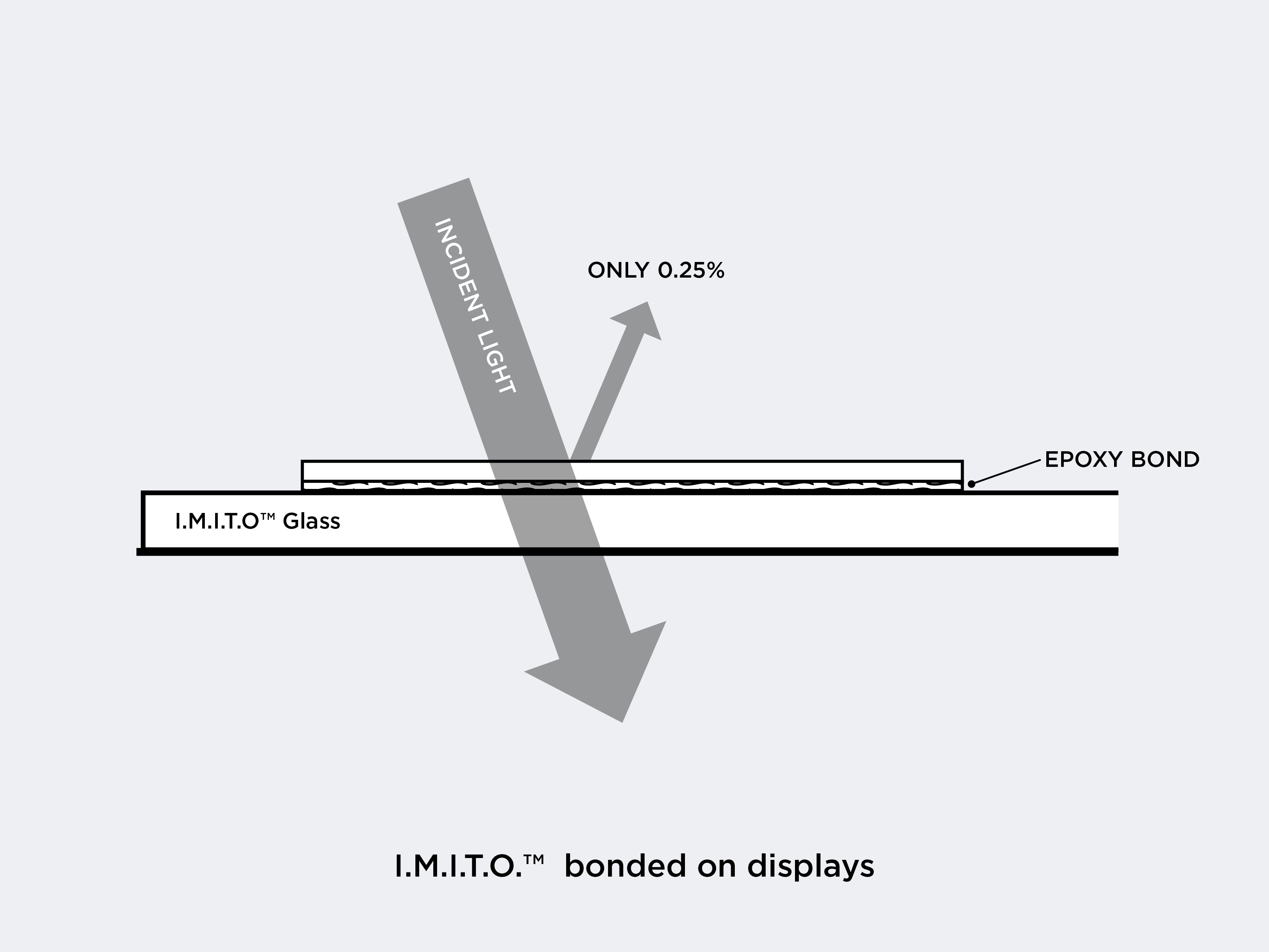
The internal reflections can be reduced to as low as 0.2-0.5% as seen in the accompanying curves. I.T.O. and I.M.ITO™ reflectivity is compared in the curves as well.
The I.M.ITO™ can be used with any of the I.T.O. resistivity’s desired, from 10 to 500 ohm/sq., but some transmission & reflection performance is sacrificed for lower resistive values of I.T.O. ≤ 10 ohm/sq.
I.M.ITO™ structure varies with the application. The I.T.O. is made as the top coat for LCD and other display usage. For E.M.I. and heater applications, the ITO is sandwiched between dielectrics to give maximum transmittance. This is also the layering used where epoxy, or oil is on that surface, as in ruggedization applications requiring lamination.
I.M.ITO™ can be patterned as small as 5 µm features for up to 14″ x 18″ sizes.
The I.M.ITO™ for LC applications is etchable by standard etchants. Thin Film Devices also provides etched panels where required, with the guarantee of “no residual” (bridges, leakage, etc.). The low surface roughness of I.M.ITO™ for LC permits cell gaps of 3mm.
| Process Method | Enhanced Magnetron Sputtering |
|---|---|
| Resistivity: | 2 - 600 ohm/sq. (Standard ITO) |
| Accuracy of value: | ± 10% of specified value (nominal) |
| Substrates: | Glass, Silicon, Quartz, Germanium and others |
| Optical Index: | Gradient (See curves Below) |
| Surface Roughness: | 7 ± 2 Å (for 1500 Å film) |
| Etch -ability | 5 µm features. |
| Uniformity: | ≤ 5% within 14“ x 14” |
| Size: | 18” x 16” 28” x 36” or smaller |
| Shapes: | Flat curved domed cupped & rod |
| Desirable ohm/sq Range | ||
|---|---|---|
| Displays | Oled TFD |
≤ 20 ≤ 20 |
| Touch Screen |
Capacitive Digital Resistive |
300 - 600 |
| Solar | PET Polymers |
≤ 20 ≤ 20 |
| Shielding | EMP EMI RFI |
≤ 4 ≤ 20 ≤ 500 |
| Heater | Not Recommended | |
| Mil C-675C | No part of coating removed by standard tape pulls. (Severe) |
|---|---|
| Mil 810C M-13508B |
No visible degradation after 3 80 eraser rubs. (Severe) |
| Mil C-675A Mil M-3508B |
Shall withstand 24 hours of 95 – 100% humidity @ 120°F. |
| M-4806A | Shall show no evidence of deterioration after exposure to ambient temperature of –65°F and 160°F for 4 hours at each specified temperature. |